Shortlist der besten Einreichungen

Der Preis für technologische Spitzenleistungen auf dem Gebiet der industriellen Bildverarbeitung wird während der VISION verliehen.
Alle fünf Unternehmen werden ihre Innovation im Rahmen einer einstündigen Session der Industrial Vision Days am 7. Oktober vorstellen. Warren Clark, Verlagsleiter von Imaging and Machine Vision Europe, dem Sponsor des mit 3.000 € dotierten Preises, wird die VISION Award Preisverleihung moderieren. Martin Wäny (CEO of TechnologiesMW SA and Photolitics OOD) wird als Mitglied der Jury am Ende die Laudatio halten und den Gesamtsieger küren.
|
Diese Unternehmen haben es in die engere Wahl für den VISION Award geschafft:





Abstracts
- PHOTODEX: Breaking the Motion Barrier in Photometric Stereo, Mobile Inspection System for Intelligent, Robust Industrial Surface Analysis
- Odem - 4D Coherent Vision on a Single Chip: Native Per-Pixel Velocity for Machine Perception
- Virtualising Machine Vision
- photonicSENS: From Plenoptic Research to Industrial 3D Vision
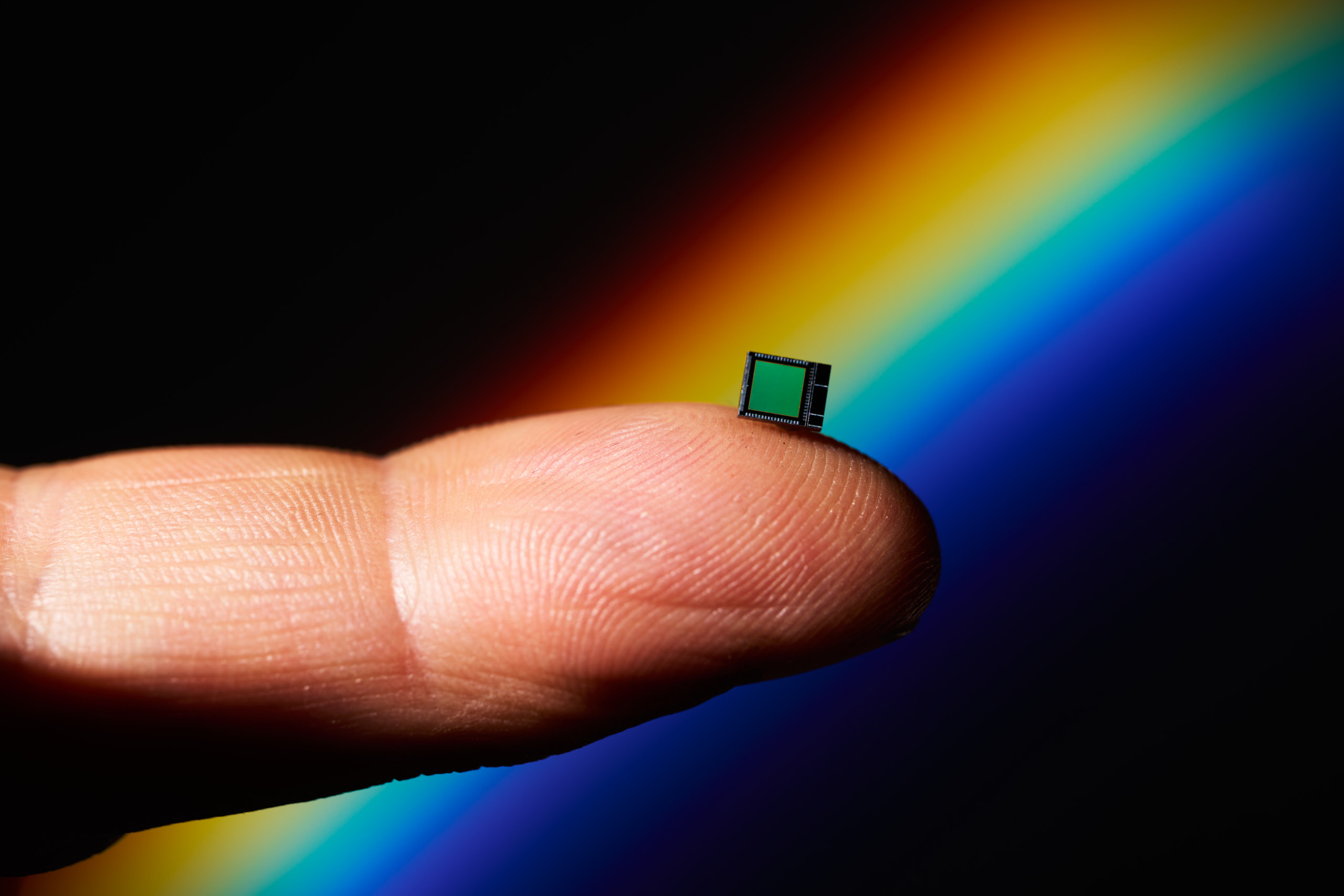
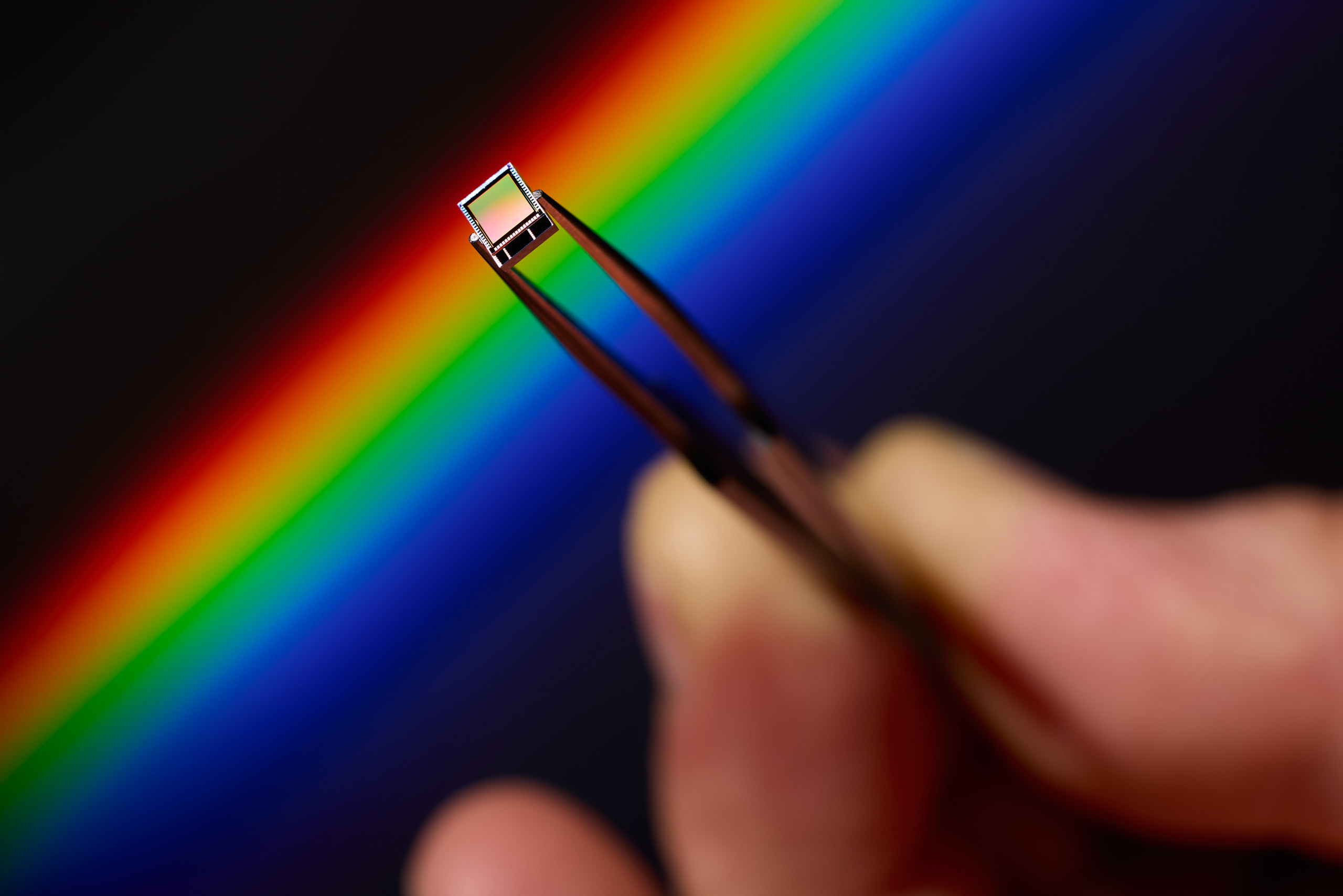
- From Light to Insight: Litavis Sensor Brings In-Pixel Processing to SPADs
Company: AIT Austrian Institute of Technology
Author: Georg Kaniak, Tamas Magyar, Ernst Bodenstorfer, Petra Thanner
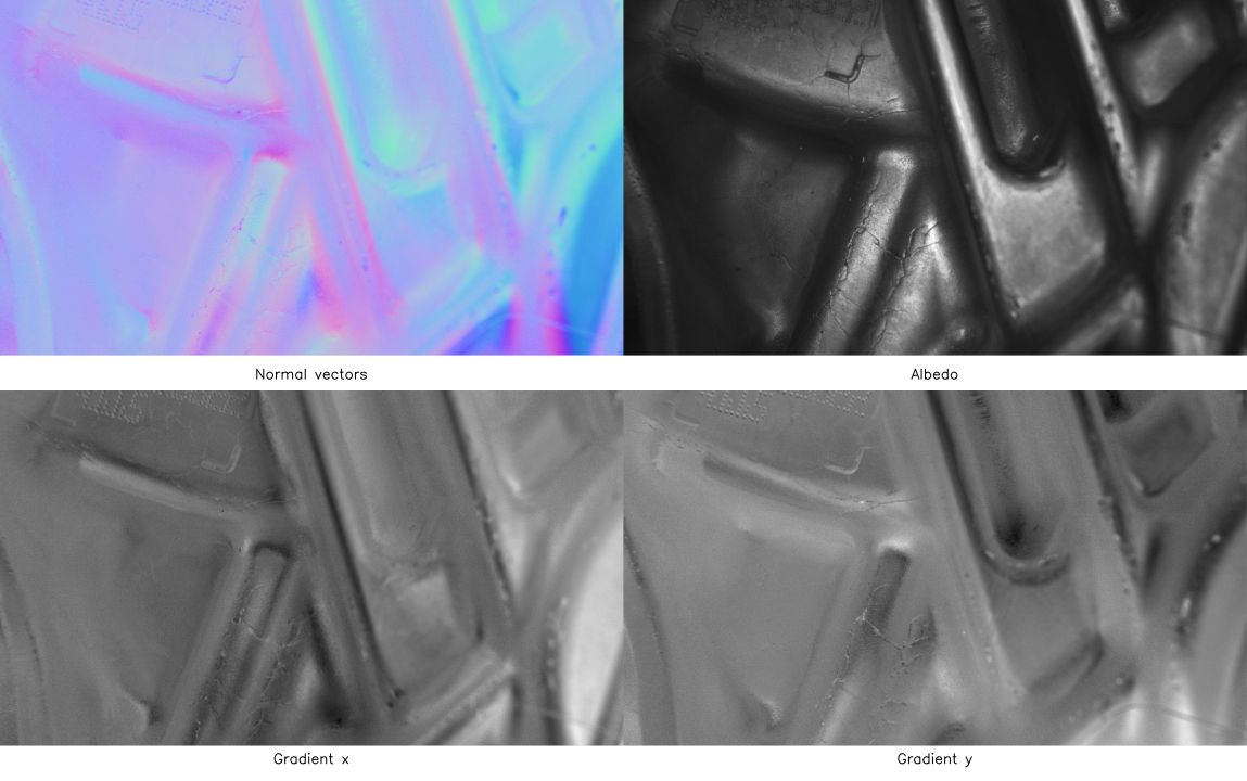
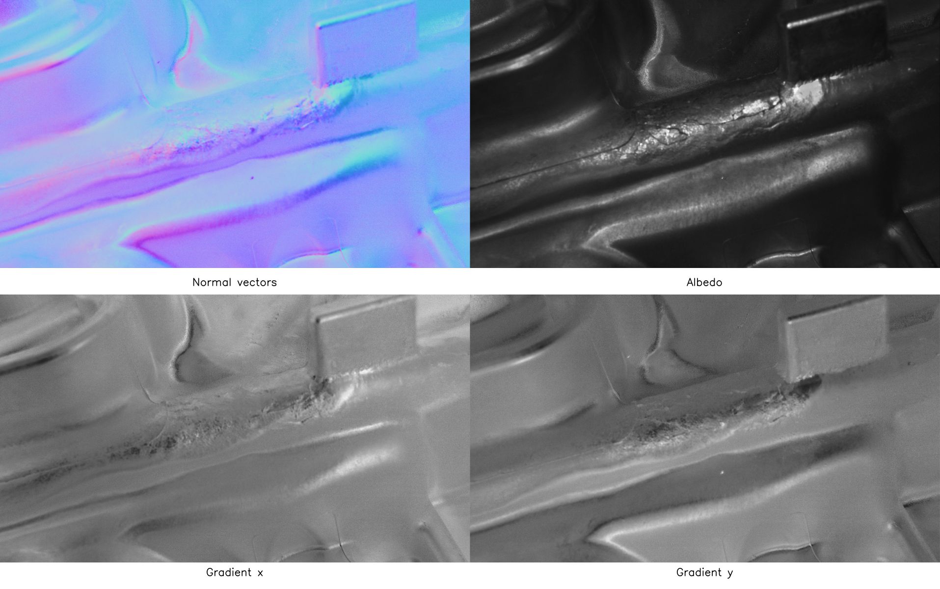
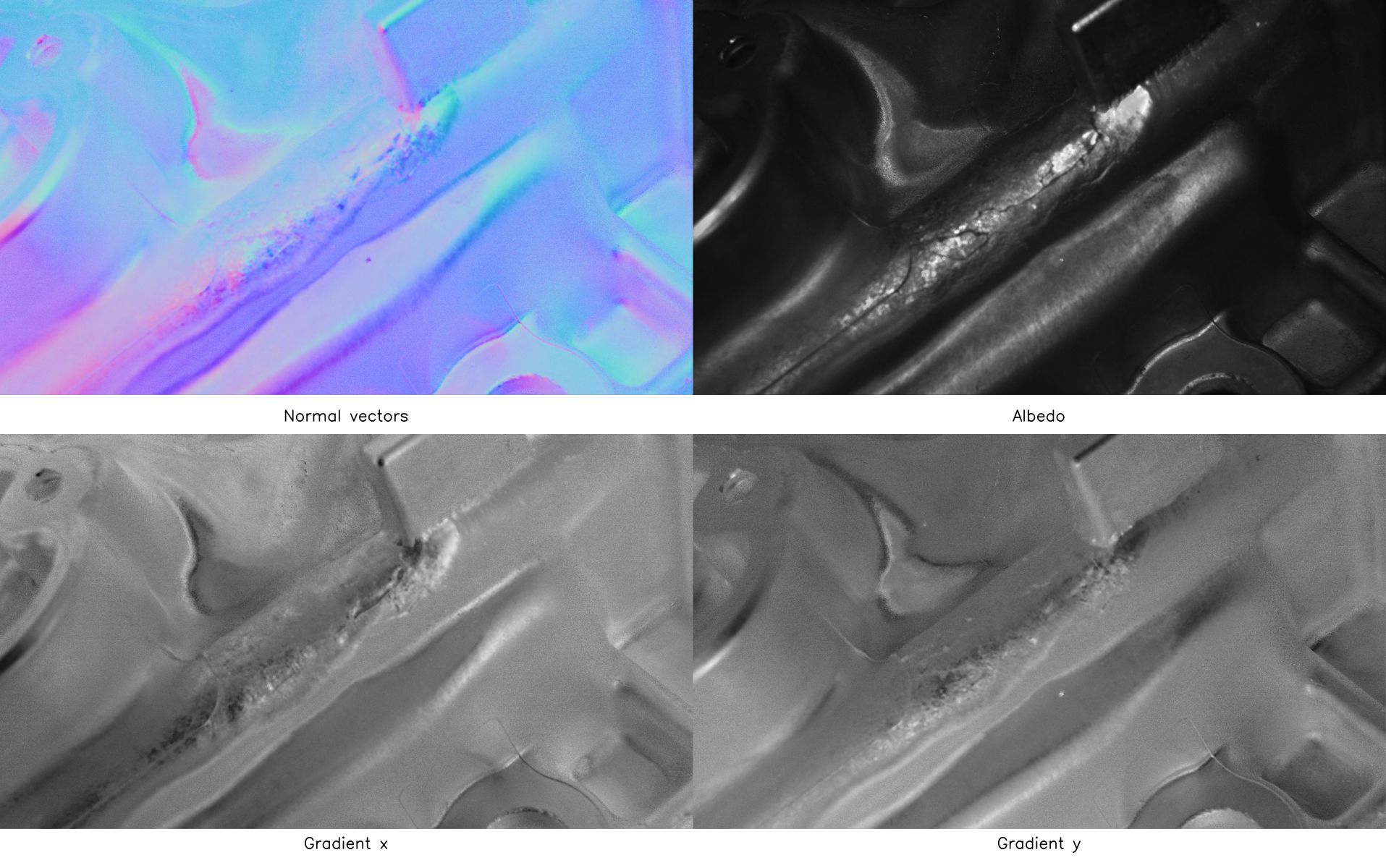
Traditional photometric stereo (PS) is highly effective at revealing fine surface defects such as scratches, cracks, dents, texture variations, and material inconsistencies that are often invisible to conventional 2D imaging and difficult to capture with standard 3D sensors.
However, existing PS systems require multiple sequential images under different lighting conditions, making them sensitive to motion and restricting their use to stationary laboratory setups or stop-and-go inspection processes.
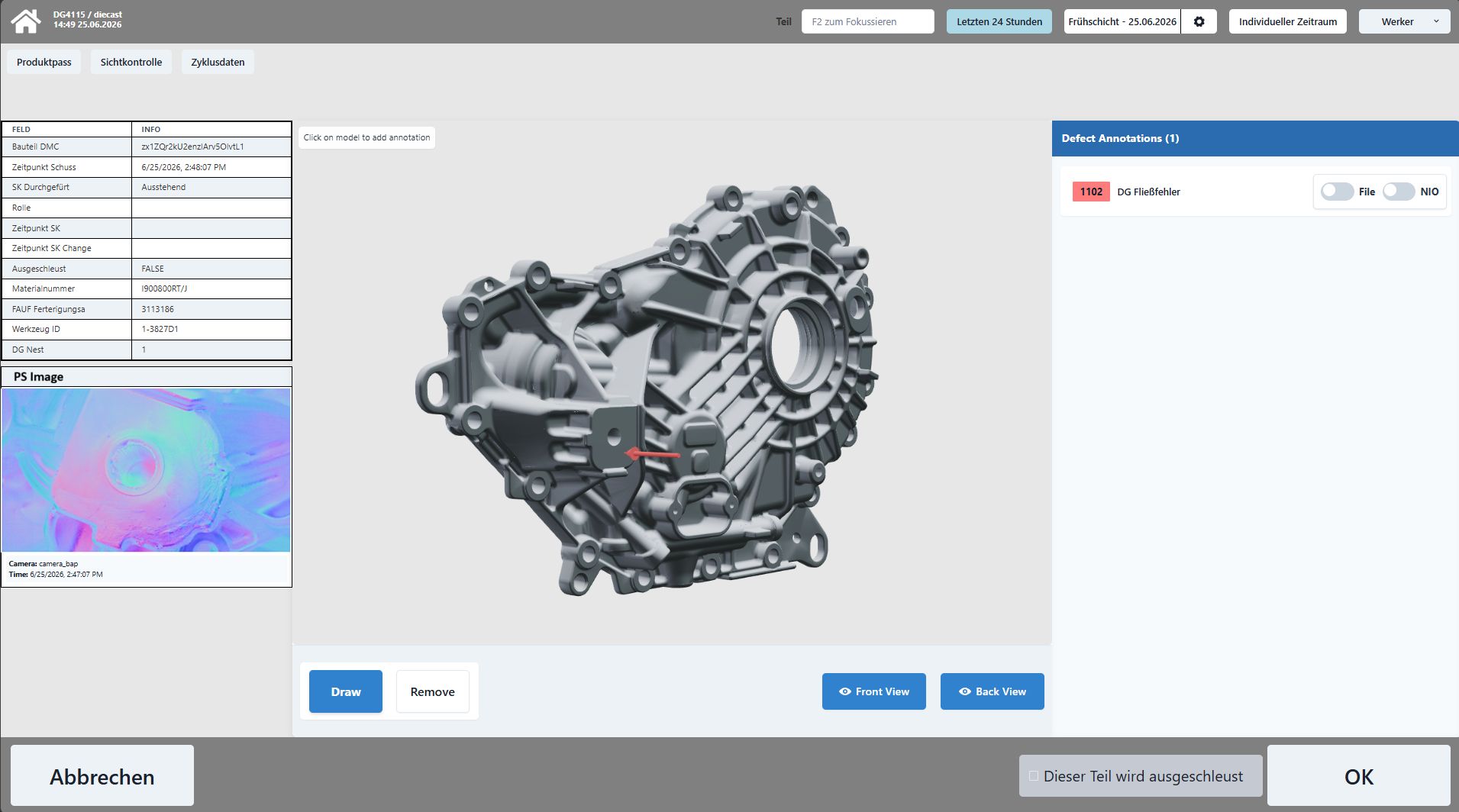
PHOTODEX overcomes this limitation through high-speed imaging and bright color-coded strobing illumination that capture the required photometric information in only two closely spaced exposures,creating a quasi single-shot photometric stereo process. This enables reliable high-resolution surface inspection during continuous handheld or robotic movement without introducing motion artifacts. A key innovation is the simultaneous determination of the camera pose relative to a known CAD model. Every captured image is automatically registered to the corresponding digital twin, allowing detected defects to be precisely localized and documented within a spatially referenced digital environment. This transforms inspection results into structured data that can be directly integrated into engineering, quality management, and manufacturing workflows.
Compared with conventional structured-light or 3D inspection systems, PHOTODEX preserves full spatial resolution during continuous scanning while providing detailed photometric surface information in addition to geometric data. Existing alternatives often require reduced resolution to maintain industrial inspection speeds and generally lack the ability to capture the fine surface characteristics revealed by photometric stereo.
The system enables both handheld inspection of large or difficult-to-access components and continuous robotic inspection without stop-and-go motion. By automatically linking detected defects to their exact position on the digital twin, PHOTODEX significantly improves defect traceability, documentation, and root-cause analysis. An additional benefit is the automatic creation of standardized, spatially referenced ground-truth datasets for AI applications. Defects can be annotated directly on the CAD model, reducing manual inspection and labeling effort while accelerating the development and deployment of AI-based quality assurance systems.
Typical applications include inspection of die-cast and forged components, die-casting molds, automotive body parts, battery housings, structural castings, and aerospace components. Manufacturers benefit from shorter inspection times, lower inspection costs, reduced scrap and rework, improved product quality, higher throughput, and seamless integration into digital engineering environments.
By integrating high-resolution surface inspection, motion-robust photometric stereo, digital twin localization, and AI-ready data generation into a portable platform, PHOTODEX removes a long-standing barrier to mobile industrial inspection and establishes a unified workflow for surface characterization, defect localization, and digital quality assurance.
Technical details and advantages of the innovation:
In many industrial sectors, defect inspection and documentation still rely heavily on manual visual assessment. Although defects are detected, essential information such as defect type, exact location, and surface characteristics often remains undocumented in digital form. This limits traceability, root-cause analysis, and the generation of high-quality datasets for AI-based inspection.
Photometric stereo (PS) is a well-established technique for reconstructing fine surface details from images captured under different illumination directions. It reveals surface features such as scratches, dents, cracks, texture variations, and material inconsistencies that both conventional 2D images or 3D sensors cannot detect. However, existing PS systems require multiple sequential images acquired under varying lighting conditions. As a result, both the camera and the object must remain stationary, restricting deployment to laboratory environments, fixed installations, or stop-and-go robotic inspection.
This limitation becomes particularly critical for handheld and continuous robotic inspection, where even slight motion between exposures degrades reconstruction quality. Existing solutions therefore require a compromise between image quality, acquisition speed, and motion robustness.
PHOTODEX, developed by the AIT Austrian Institute of Technology, overcomes this limitation by combining high-speed imaging with bright, color-coded strobing illumination. All photometric information is captured in two consecutive exposures with minimal temporal separation, effectively creating a quasi single-shot photometric stereo acquisition. This enables high-resolution Surface inspection during continuous handheld or robotic motion without compromising measurement quality. At the same time, the system determines the camera pose relative to an object with a known CAD model.
Every image is automatically registered to the digital twin, allowing precise localization of surface defects and seamless integration into digital engineering workflows. Compared with existing 3D inspection systems, PHOTODEX uniquely combines high-resolution surface characterization with accurate CAD-referenced localization in a compact portable device. While commercial structured-light systems can inspect moving objects, maintaining industrial inspection speeds typically requires a significant reduction in spatial resolution--often by approximately a factor of three.
Moreover, these systems provide only geometric information and cannot capture the fine Surface characteristics revealed by photometric stereo.
PHOTODEX preserves full spatial resolution while simultaneously delivering detailed photometric Surface information and precise CAD-based localization. This enables applications that are difficult or impossible with existing technologies, including handheld inspection of large components, continuous robotic scanning without stop-and-go motion, and intuitive localization of defects directly on the digital twin.
The key advantages are:
- Portable handheld and robotic operation: enables flexible inspection of large or difficult-to-access components.
- Quasi single-shot photometric stereo: eliminates motion artifacts caused by sequential image acquisition.
- High spatial resolution: maintains full resolution during continuous scanning.
- Simultaneous CAD-based localization: directly registers every measurement to the digital twin.
- Improved defect traceability: automatically links detected defects to their exact position on the digital twin.
By integrating motion-robust photometric stereo, high-resolution surface inspection, and digital twin localization into a single portable system, PHOTODEX removes a long-standing barrier to deploying photometric stereo in truly mobile industrial inspection. This enables manufacturers to inspect larger components faster, reduce inspection effort and integrate high-resolution surface information directly into digital quality workflows.
Relevance and application possibilities of the described innovation for the machine vision industry:
Manufacturers are facing increasing pressure to improve product quality while reducing costs, material waste and inspection effort. Growing component sizes, complex geometries and shorter production cycles are driving demand for faster, more reliable inspection solutions. At the same time, the shortage of skilled workers and the rapid adoption of AI are driving demand for standardized, spatially referenced ground-truth data for AI-based quality assurance.
PHOTODEX tackles both challenges by combining high-resolution surface inspection with automated spatial defect annotation. The system reveals surface structures beyond the capabilities of conventional 3D sensors while generating structured defect information, including the exact location of every detected defect. Unlike conventional inspection systems, PHOTODEX automatically generates standardized, spatially referenced ground-truth datasets that enable AI-driven inspection. The standardized spatially referenced datasets improve traceability, simplify root-cause analysis and accelerate the deployment of AI-based inspection and decision-support systems. By combining quasi single-shot photometric stereo with CAD-based localization, PHOTODEX bridges the gap between detailed surface characterization and digital twin integration, transforming photometric stereo from a laboratory method into a practical industrial inspection technology.
A key application is the inspection and annotation of surface defects on die-cast and forged components, where even small defects can lead to costly scrap, rework or tool adjustments. Creating training data for automated defect detection is still labor-intensive, as experts manually inspect and document defects such as cracks, cold shuts, scratches, porosity marks and inclusions. PHOTODEX automatically registers every detected defect to the CAD model, enabling annotation directly on the digital twin and creating standardized, spatially referenced ground-truth datasets for AI training. Manufacturers benefit from lower inspection and annotation effort, standardized defect documentation, faster root-cause analysis, accelerated AI deployment, lower scrap rates and higher product quality.
A second application is the robotic inspection of large components such as die-casting moulds, automotive body parts, battery housings, structural castings and aerospace components.
PHOTODEX enables continuous robotic scanning while maintaining full spatial resolution, reducing inspection time, robot commissioning effort and downtime while increasing throughput. Every measurement is automatically linked to the CAD model, enabling seamless integration into digital engineering and quality management workflows.
Beyond these applications, PHOTODEX supports several key trends in machine vision:
- Digital twin integration: Every inspection result is directly linked to the CAD model.
- AI-ready datasets: Standardized, spatially referenced annotations facilitate machine learning.
- Mobile machine vision: High-resolution photometric stereo becomes practical outside fixed inspection cells.
- Scalable automation: One technology that supports both handheld and robotic inspection.
- Improved traceability: Defects can be precisely localized and tracked throughout the product lifecycle by automatically registering them to the digital twin, ensuring full traceability.
- Higher productivity: Continuous scanning eliminates stop-and-go inspection procedures.
By combining established sensing technologies in a novel way, PHOTODEX removes the motion constraints that have long limited industrial photometric stereo and transforms it into a practical industrial inspection technology. The result is a portable, high-resolution, spatially aware inspection system that integrates seamlessly with digital engineering workflows.
This establishes a new paradigm in which surface characterization, defect localization, and digital twin integration become a single, unified process enabling shorter inspection times, lower inspection costs,reduced scrap, higher product quality and faster deployment of AI-powered quality assurance across industries such as automotive, battery manufacturing, die casting and aerospace.
Unique Selling Point (USP):
PHOTODEX is the first portable inspection system combining motion-robust photometric stereo, high-resolution surface inspection, CAD-based defect localization and AI-ready annotation. It transforms photometric stereo into an industrial technology for continuous handheld and robotic inspection, automatically linking defects to the digital twin for AI-driven quality assurance.
When will the innovation be available?
PHOTODEX is available today for collaborative R&D projects involving high-resolution photometric stereo imaging and 3D defect annotation.

Company: Lidwave
Author: Eyal Assa
Every conventional vision system, cameras and pulsed LiDAR alike, captures geometry. To understand whether something is moving, the system must compare frames over time and infer motion through computation. That inference is slow, fragile under poor lighting, and breaks down in fog, dust, spray, and direct sunlight.
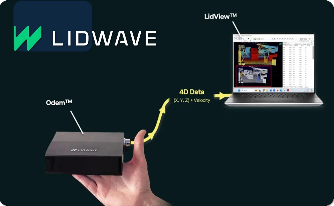
Odem removes the inference step. Built on Lidwave's patented Finite Coherent Ranging (FCR(TM)) technology, Odem is a 4D coherent vision sensor that measures range, reflectivity, and instantaneous velocity (Doppler) for every single pixel, in the same optical instant. Velocity is no longer estimated, it is measured natively, as a fourth data dimension delivered directly from the sensor. The entire optical engine: laser, amplifiers, and detectors, is integrated onto a single silicon chip in a true monostatic architecture, where each channel both transmits and receives. The result is a calibration-free, vibration and temperature-resilient sensor that streams millions of depth-and-velocity points per second over hundreds of meters, and that can be manufactured at wafer scale. Odem is the first vision sensor to measure true instantaneous velocity at every pixel - optically and in real time - on a single, calibration-free silicon chip. It turns motion from something machine vision computes into something the sensor sees, delivering range, reflectivity, and Doppler velocity in one robust device that is manufacturable at a scale conventional LiDAR cannot match.
Technical details and advantages of the innovation:
1. Coherent FMCW sensing (based on our unique FCR(TM)): Each pixel emits an optical signal with unique phase and frequency manipulations, and mixes the return against a local reference arm. The beat frequency yields range and Doppler velocity simultaneously - no frame stitching, no motion estimation, no post-processing.
2. True single-chip monostatic design: Laser, amplification, and detection are integrated on one photonic chip, with transmit and receive co-located at the every channel. This eliminates the multi-component optical alignment that limits conventional LiDAR.
3. Calibration-free operation: Because there is no separate transmit/receive optical path to align, the sensor requires no field or factory calibration - enabling streamlined, large-scale production and drastically lower unit cost at volume.
4. Coherent rejection of interference: As a coherent receiver, Odem is intrinsically immune to ambient light, sunlight saturation, and cross-talk from other sensors, and it maintains clean depth and velocity data through rain, fog, dust, and snow.
5. Mechanical robustness: The monolithic design delivers high resilience to vibration and temperature swings without performance loss - critical for moving platforms and industrial environments.
6. Rich native data stream: Range + reflectivity + per-pixel instantaneous velocity, at millions of points per second, over hundreds of meters.
Relevance and application possibilities of the described innovation for the machine vision industry:
Per-pixel velocity reshapes the hardest problems in machine vision. Real-time segmentation becomes trivial when moving and static objects are separated by their measured Doppler signature rather than by frame-to-frame computation - slashing the perception compute load that today's AI-driven vision systems struggle with.
For robotics and embedded vision (AMRs, AGVs, drones, humanoids), Odem gives the platform an immediate, lighting-independent understanding of what is moving and how fast, enabling safe high-speed operation where camera-only stacks fail.
In industrial automation and in-line inspection, the same sensor delivers high-resolution 3D geometry and instantaneous motion in one device, supporting bin-picking, conveyor and high-speed process monitoring, and dimensional measurement of objects in motion. Its robustness to dust, mist, and glare opens harsh-environment applications - logistics yards, ports, agriculture, construction, and outdoor robotics - that conventional machine vision cannot reliably serve. And because it produces clean raw data without fusing multiple sensors, Odem simplifies system architecture and reduces the integration burden across the entire vision stack.
This is the data layer that physical AI has been missing: not just where things are, but how the scene is moving - measured, not inferred.
Unique Selling Point (USP):
Odem is the first vision sensor to measure true instantaneous velocity at every pixel - optically and in real time - on a single, calibration-free silicon chip. It turns motion from something machine vision computes into something the sensor sees, delivering range, reflectivity, and Doppler velocity in one robust device that is manufacturable at a scale conventional LiDAR cannot match.
When will the innovation be available?
Odem 2.5 engineering samples are shipping to evaluation partners today, production grade Odem 3 is scheduled for 2027.
Company: Medabsy GmbH
Author: Trang Nguyen
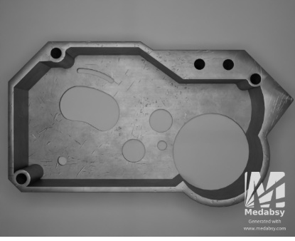
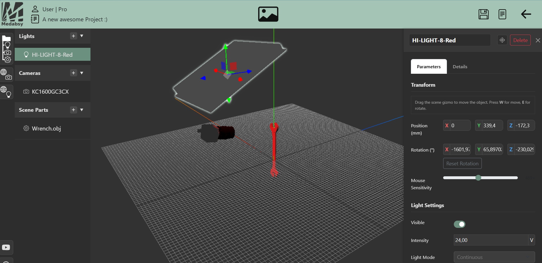
Medabsy is a CAD platform for designing machine vision systems -- the cameras and lighting that automatically inspect products on factory lines. Today they are largely designed by trial and error; Medabsy replaces guesswork with simulation. In our editor, the user imports a 3D model of their part and defines its material, texture, and the target surface defects, all derived from physical parameters. The inspection setup can be planned manually or with our optimization algorithm, using a database of market-available components. We then run physically accurate light simulation to generate synthetic datasets -- with pixel-perfect defect masks, full control over content, and rare edge cases on demand. This matters because real defect samples are scarce and hard to collect, yet reliable inspection AI depends on large, controlled, well-labeled training data.
Technical details and advantages of the innovation:
Currently, experts perform the inspection design manually in a lab by rearranging imaging hardware and assessing performance which can take weeks.
With Medabsy, the customer can design the digital twin of the inspection system on their own, by loading a 3D model of the inspected product, choosing components from hardware library and simulating the results.
The digital twin is further used for bill of materials, system specification and synthetic data Generation.
AI needs 1000s of labelled training images, which are not available for inspection - developers are lucky if they get 300 labelled images! And the dataset they get usually lacks the examples of the hardest defects.
Currently, the few available images are multiplied, by introducing rotation, perspective and color transformations - however, the defect still stays the same, no new information is obtained. With Medabsy, the customer can generate as many training images as they need! With each new image providing new appearance information. On their own, user can control surface appearance, dirt, defect characteristics and simulate any common or edge-case scenario they can think of.
Many are trying to use generative AI for synthetic data generation - however, pixel precise labelling is very difficult, and it is impossible to guarantee for the dataset content due to network hallucination.
Medabsy's synthetic images are generated using Monte Carlo simulation and stochastic geometry modelling for texture and defects. This means that the user has complete control over the results, knowing exactly which content is going to be generated for a given set of Parameters.
Added Value Proposition
- Sales efficiency increase
- Early risk assessment and cost planning
- Avoid penalties - stress test before deployment
- Train AI before having real data
- Train for edge-case scenarios
Relevance and application possibilities of the described innovation for the machine vision industry:
Using Medabsy software platform, it is possible to
* speed up inspection system design by 40% by designing and simulating inspection results virtually
* speed up AI project by 94% by using synthetic datasets
* simulate critical defects and edge cases which rarely occur in production
* simulate hardware performance before ordering hardware components
* quickly estimate inspection feasibility
* simulate a wide variety of defects using physical parameters such as type, width, depth, location (e.g. 0.2 mm wide crack, 2mm deep with branching)
* control texture parameters created by production process (milling, turning, casting...)
It is already tested by customers.
Unique Selling Point (USP):
Our software lets users virtually design machine-vision systems using real market-ready hardware, then generate photorealistic synthetic training data with pixel-perfect annotations. Unlike generative-AI tools, we create datasets via physical light-transport simulation and mathematical texture/defect models--no generative AI--ensuring physical accuracy, full controllability, and systematic coverage.

Company: PhotonicSENS
Author: Sergio Mantecón, Chief Commercial Officer, photonicSENS S.L.
Plenoptic imaging has been understood theoretically since the early 20th century. The physics are well established. What has been missing, until now, is a manufacturable, calibrated, industrially deployable implementation at a price point that makes it viable outside a research budget.
photonicSENS was founded in Valencia in 2015 with the specific aim of closing that gap. The company has developed a proprietary plenoptic (light field) camera platform that captures a full 2D image and a high-resolution depth map simultaneously, from a single sensor, in a single shot, in real time. There is no projected pattern, no second exposure, no external projector, and no on-site calibration procedure. The camera ships calibrated and outputs metric depth immediately.
The optical principle is straightforward to describe, though demanding to manufacture. A Micro-Lens Array (MLA) is positioned between the main imaging lens and the image sensor. The MLA enables to reconstruct multiple slightly different angular perspectives of the scene, encoding directional as well as spatial information into a single raw frame. This four-dimensional light field is then processed by a proprietary epipolar analysis algorithm that extracts per-pixel depth from the angular shift between adjacent sub-aperture views, without iterative correspondence search, and without the failure modes that affect stereo matching on repetitive or textureless surfaces.
The depth values that come out are measured, not inferred. Every reported point in the depth map corresponds to a genuine angular parallax measurement. The 2D image and depth map are inherently co-registered at pixel level, not because they have been aligned in post-processing, but because they come from the same optical path at the same instant. One of photonicSENS's key strengths is the engineering effort invested in an ultra-efficient implementation of the depth-estimation algorithms. Years of optimisation have brought the processing pipeline to the point where it delivers real-time point clouds on a compact, self-contained system, without the powerful and expensive workstations or GPU clusters that comparable 3D approaches typically demand. This efficiency is what makes the embedded SMART line possible and what keeps total cost of ownership within reach for industrial deployment.
Making this work reliably at industrial scale required solving a manufacturing problem that has no off-the-shelf solution. Assembly of a light field camera demands sub-micrometre alignment between the MLA and the image sensor. photonicSENS developed a fully automated, proprietary assembly process using six-axis active alignment with real-time image quality feedback, implemented in a dedicated cleanroom facility in Paterna, Valencia (Spain). Each camera is individually calibrated against traceable reference targets to establish the pixel-to-depth relationship: a one-time factory process that holds for the operational life of the camera without further adjustment on site.
Most machine vision sensors require in-situ calibration as part of every system installation. photonicSENS cameras do not.
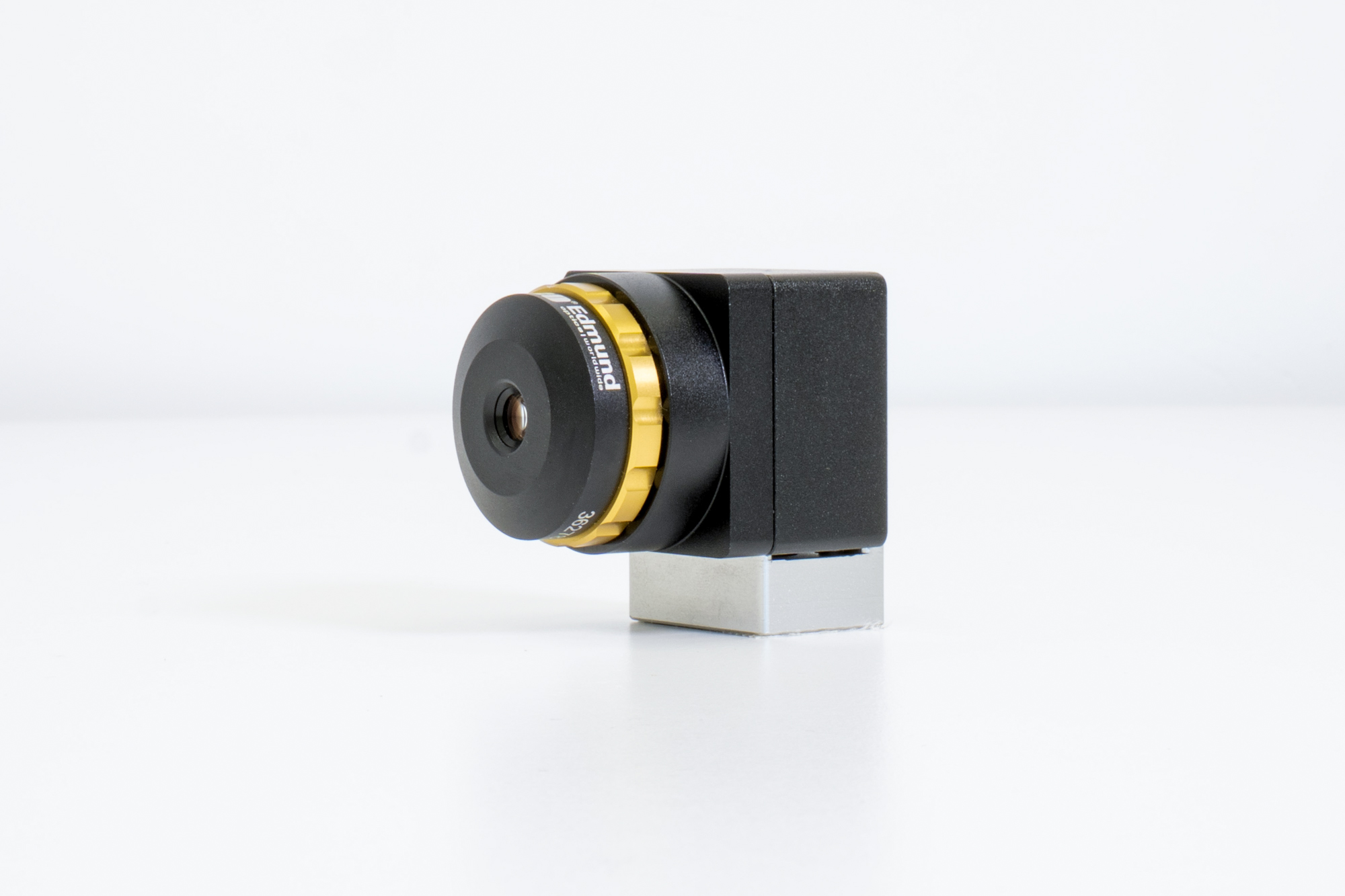
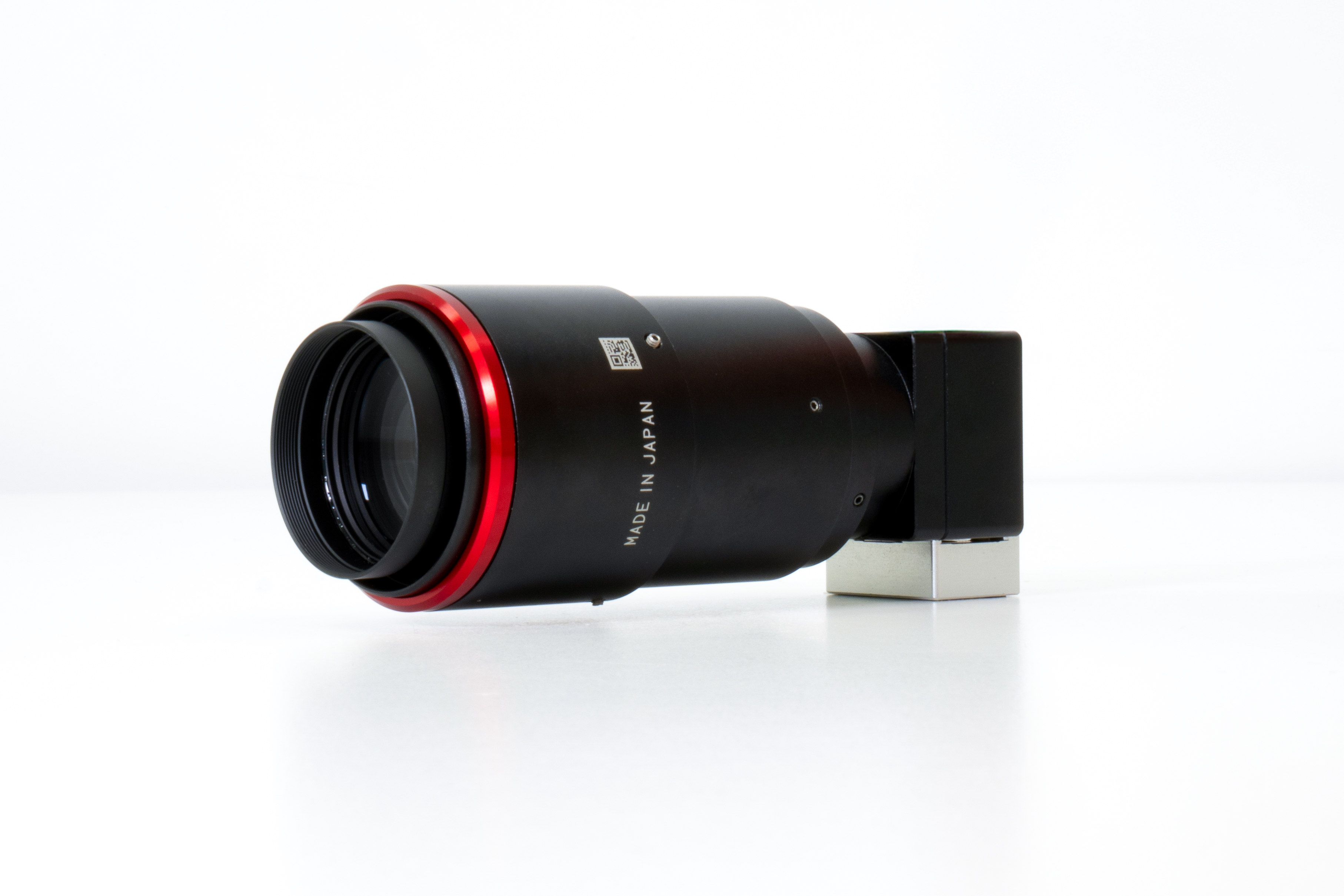
The resulting product portfolio spans eight camera families (MICRO through VIVID+), covering depth precision from 0.6 µm to the millimetre range, with 1.4 and 2.1 megapixel depth maps and fields of view from under 2 mm to over 100 mm diagonal. The most recent addition to the range is the apiCAM SMART series, which integrates the full acquisition and depth-processing pipeline into an embedded industrial camera body. All computation runs onboard. The output is a calibrated 2D image and metric depth map, delivered over Ethernet with GenICam compatibility, external trigger support, and optional IP65 protection. No external PC, no GPU cluster, no specialist infrastructure.
A portfolio of granted patents covers the MLA optical design, the depth estimation method, and the manufacturing assembly process. A superresolution algorithm developed in-house reduces the spatial resolution penalty inherent to light field imaging by a factor of N rather than N², partially recovering the resolution trade-off that is the technology's principal limitation.
Technical details and advantages of the innovation:
The dominant 3D sensing methods in industrial machine vision, structured light projection, laser line triangulation, stereo vision, and time-of-flight, each carry constraints that are well understood by anyone who has tried to apply them at the boundary of what they can do.
Structured light systems need multiple exposures and a projector in the optical path. They work well in controlled conditions, but single-shot capture of moving targets is not possible, and specular or transparent surfaces cause the projected pattern to break down. Laser line triangulators require a scan axis, which limits throughput and rules them out wherever a static single-shot acquisition is needed. Time-of-flight sensors are fast and cover long ranges, but close-range precision is limited and multipath interference on reflective surfaces introduces systematic errors. Stereo vision requires two mechanically stable, thermally calibrated optical paths and correspondence algorithms that fail predictably on
textureless areas and repetitive patterns.
What none of these methods delivers is a true per-pixel depth map from a single shot, from a single compact sensor, with the depth and 2D data inherently aligned. Light field imaging delivers exactly that, which is why it has attracted sustained research interest for twenty years. The reason it has not previously appeared in production environments is the manufacturing difficulty described above, combined with the computational cost of earlier processing approaches.
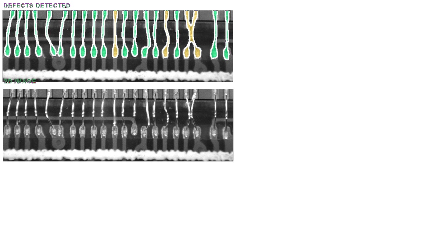
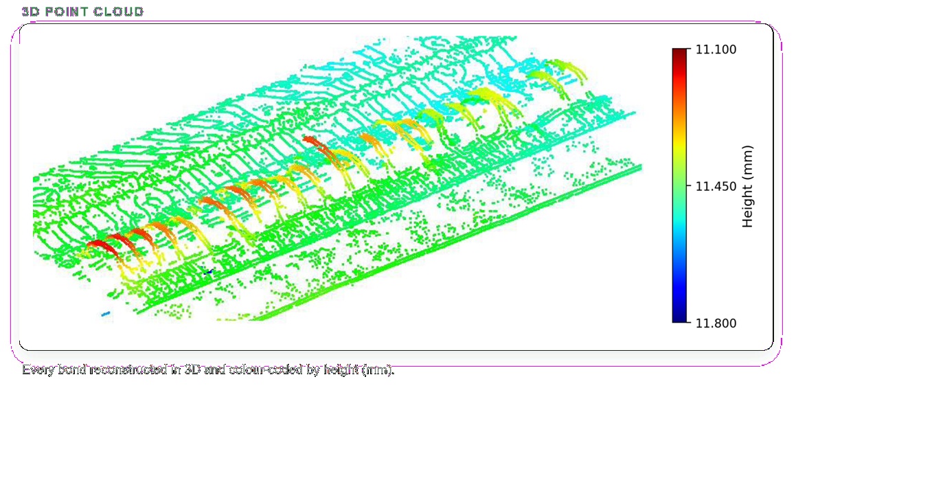
photonicSENS has addressed both. The manufacturing process exists, is automated, and is running. The processing pipeline is efficient enough for real-time operation on standard GPU hardware, and has been further reduced to embedded implementation in the SMART product line. On surfaces where established 3D methods struggle most, the advantages are concrete. Highly polished metallic components, machined screws, connectors, milled fasteners, produce specular reflection artefacts in laser profilometers: data voids, ghost points, degraded accuracy. The passive light field approach, combined with appropriate illumination, produces reliable depth data on these surfaces, enabling geometrical model fitting to detect dimensional deviations below 10 µm. On transparent substrates such as cover glass or optical windows, depth-based classification separates genuine surface defects from dust and foreign objects, something 2D imaging cannot address and most 3D methods handle poorly. In microelectronics assembly, the combination of 2.1 megapixel depth resolution at 2.4 µm precision and single-shot capture supports inline 3D metrology of wire bonds and solder joints at production cycle rates.
Light field imaging does have genuine limitations: Performance is strongest at short working distances and compact fields of view: the physics of the disparity-depth relationship mean that precision degrades with distance, and field of view and depth range trade off against each other within a given optical configuration. For applications requiring large fields of view, long working distances, or sub-micrometre precision at scale, other methods are often more appropriate. The photonicSENS contribution is not to claim the technology works everywhere. It is to make it work reliably where it is the right choice, and to provide sufficient portfolio range to address the majority of precision inspection scenarios that fall within its envelope.
Relevance and application possibilities of the described innovation for the machine vision industry:
The machine vision industry is well served by mature, proven 3D sensing technologies. What it has lacked is a commercially available light field option: a sensor that delivers true single-shot depth without a projector, without a scan axis, and without post-hoc registration between the 2D and 3D data streams. photonicSENS fills that gap.
For system integrators, a calibrated photonicSENS camera arrives ready to output metric depth. The SDK supports Python, MATLAB, LabVIEW, and Halcon, with full GenICam compliance in the SMART line. There is no alignment step between the 2D image and depth map because there is no alignment to do.
Applications that previously required a structured light projector and a 2D camera, two components to mount, calibrate, and maintain, can now be addressed with a single sensor. For OEMs and integrators working in space-constrained environments, this is a real simplification. The SILICON project, co-funded by the European Union under the ERDF Comunitat Valenciana 2021-2027 programme, provided independent third-party validation of the photonicSENS approach against established 3D solutions across agricultural sorting and automotive inspection use cases. The project confirmed performance and delivered hardware improvements including a reduction in energy consumption exceeding 50% and significant cost reduction relative to prior configurations.
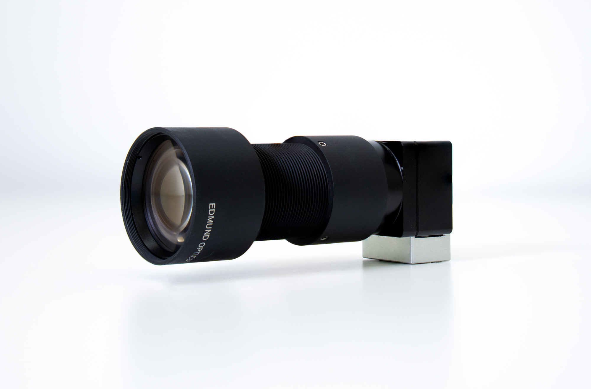
Application areas include wire bonding inspection in semiconductor packaging and PCB solder joint volume measurement. In wire bonding, bonds as fine as 20 µm are reconstructed cleanly, allowing verification that each bond is correctly attached to the wedge and that the height and shape of the wire matches specification. Glue bead continuity and geometry verification, thread pitch measurement on fasteners, and surface and subsurface defect classification on transparent components are further demonstrated use cases. In pharmaceutical manufacturing, a live production demo with Edmund Optics at MedtecLIVE Stuttgart in 2026 detected engraved tablet markings at under 100 µm depth, outputting simultaneous 2D and 3D data in a compact, line-ready form factor. The compact form factor and low weight also make the cameras well suited to mounting on a robotic arm, opening up emerging applications under active development: robotic bin-picking of metal components, inspection of additively manufactured medical implants, and large-area inspection through X-Y-Z stitching.
The 2026 product roadmap includes global shutter sensor integration, removing the current constraint on fast-moving targets, extended depth range configurations, and full-resolution output modes. A single camera, a single shot, a calibrated depth map, ready to use. Light field imaging has been discussed at VISION for years. photonicSENS is the company that has made it a product.
Unique Selling Point (USP):
The only camera that captures a full 2D image and a metric, per-pixel depth map in a single shot, from a single sensor, with zero projector, zero scan axis, and zero on-site calibration. Every depth point is a real angular measurement, not an inference. Factory-calibrated for life, running in real time on embedded hardware.
When will the innovation be available?
Available now. The core apiCAM platform (eight camera families) is in production and shipping. The SMART line is available in select models, with the global shutter variant launching Q3 2026.
Company: Singular Photonics
Author: Shahida Imani, CEO, Singular Photonics
Litavis is a next-generation single-photon avalanche diode (SPAD) image sensor designed to bring unprecedented flexibility and intelligence to advanced imaging and machine vision applications.
While conventional image sensors primarily capture intensity information and are typically optimised for a single operating mode or application, Litavis introduces a software-configurable sensing architecture capable of combining photon-counting imaging, programmable time gating, and advanced photon timing within a scalable SPAD array platform.
By combining highly sensitive single-photon detection with embedded on-chip digital photon processing, Litavis enables simultaneous high-sensitivity photon-counting imaging with time-resolved photon sensing for machine vision and LiDAR applications. The system also enables users to dynamically adapt sensor behaviour in software without requiring new hardware designs. By processing photon events directly on-chip, Litavis significantly reduces the amount of raw data that must be transferred and processed externally. This enables faster decision-making, lower latency, improved power efficiency and more scalable real-time imaging systems. Litavis represents a shift from fixed-function image sensors toward software-defined Imaging architectures. Developers can reconfigure the same hardware platform for different applications with minimal redesign effort, accelerating development cycles and reducing system complexity. Ultimately, Litavis demonstrates how computational SPAD sensors can evolve beyond the passive image acquisition towards intelligent sensing platforms that extract rich information directly from the focal plane.
Technical details and advantages of the innovation:
Litavis is a CMOS SPAD-based imaging sensor platform built on an architecture that combines single-photon sensitivity with integrated digital photon processing directly on-chip and in-pixel. This enables precise capture of spatial and temporal information, while reducing reliance on external processing hardware, allowing the sensor to extract additional scene information including depth, timing and event characteristics.
Litavis delivers continuous 256×256-pixel photon-counting imaging using 14-bit counters, delivering high-dynamic-range imaging under low-light conditions. In parallel, time-stamped photon events are generated from every pixel at kilohertz-scale rates on a reduced 64×64 grid, enabling picosecond resolution photon timing while maintaining full-resolution counting. Beyond conventional imaging, Litavis supports programmable time-windowed operation, where detection gates are selectively positioned relative to an illumination pulse. This enables depth-selective LiDAR sensing by mapping temporal gates directly to time-of-flight distance slices, while improving background rejection in scattering environments. Integrated VCSEL control enables tightly synchronised active illumination for pulsed LiDAR and structured time-of-flight imaging.
Litavis also supports multi-event timing, allowing multiple detected photons per excitation cycle to be individually time-binned, inter-arrival photon analysis which provides statistical information on photon dynamics, and on-chip histogramming. These capabilities provide access to temporal statistics beyond conventional intensity measurements. This supports applications such as fluorescence lifetime imaging, dynamic light scattering, and quantum sensing. The sensor integrates configurable acquisition and timing capabilities directly within the pixel array. This allows developers and system integrators to rapidly prototype, evaluate and deploy advanced imaging solutions using a single adaptable platform.
Litavis combines the sensitivity advantages of SPAD technology with the adaptability and scalability increasingly required by modern intelligent vision systems. The sensor is suitable for a broad range of applications including machine vision, robotics, depth sensing, spectroscopy, scientific imaging, medical imaging, quantum technologies and industrial automation.
Relevance and application possibilities of the described innovation for the machine vision industry:
As machine vision moves toward edge intelligence and real-time perception, Litavis unifies image sensing and processing on a single device, removing the off-chip processing bottleneck that limits conventional architectures.
Feature-to-application mapping:
o 14/28-bit photon counting (256×256/128) suits industrial inspection, where bright glare and dark
shadow coexist in one scene -- high dynamic range avoids saturation while preserving low-light detail in a
single exposure.
o 10s of picosecond-resolution timestamping (64×64) suits 3D depth sensing and time-of-flight imaging,
deriving range per pixel without external TDC electronics -- smaller, cheaper systems for embedded
robotics.
o Time-windowed gating with VCSEL sync suits autonomous systems in fog, dust, or smoke, rejecting
background light by gating to the illumination window -- improving range where conventional ToF
degrades.
o Multi-event timing and inter-arrival analysis suits semiconductor inspection, where fast transient optical
signals demand photon-timing statistics rather than intensity alone, enabling finer defect classification.
o On-chip histogramming and TCSPC suit life-science and medical imaging (e.g. fluorescence lifetime
imaging), where lifetime -- not brightness -- carries the diagnostic signal, removing the need for bulky
external TCSPC modules.
o Coincidence detection suits quantum and photonics applications, enabling correlated photon detection
across pixels for quantum sensing -- a capability conventional sensors lack.
o Software-defined mode switching suits traffic and mobility systems, reconfiguring for day/night or
weather conditions on one platform without hardware redesign, shortening qualification cycles.
Engineering and commercial advantages:
Because Litavis is reconfigurable in software, integrators can evaluate multiple modalities -- intensity, depth, lifetime, photon statistics -- on one platform, cutting prototyping time and de-risking development. This matters as applications converge: a robotics platform may need both conventional imaging and time-resolved depth sensing, tasks that would otherwise require two separate sensors.
By combining single-photon sensitivity, picosecond timing, and on-chip statistical processing in one CMOS-compatible platform, Litavis fills a gap in the current sensor landscape: no existing platform adapts across high-volume industrial imaging and advanced time-resolved or quantum-sensing applications without a redesign.
Unique Selling Point (USP):
Litavis is the world's first all-in-pixel, next-generation SPAD platform -- unifying imaging, timing, histogramming and photon statistics on a single chip. A paradigm shift in sensing, it collapses entire multi-sensor vision stacks into one edge-intelligent, future-proof platform -- enabling a new generation of intelligent, multi-modal vision systems built on a single, software-defined sensor.
When will the innovation be available?
September 2026